

ZHANG Nana, a postdoctoral fellow of CALM (first author), Dr. YANG Bing and professor ZHENG Hongyu (corresponding authors) have published an article entitled Near-Interface Defects in Graphene/H-BN In-Plane HeteroStructures: Insights Into the Interfacial Thermal Transport” in Nanomaterials.
Based on nonequilibrium molecular dynamics (NEMD) and nonequilibrium Green's function simulations, the interfacial thermal conductance (ITC) of graphene/h-BN in-plane heterostructures with near-interface defects (monovacancy defects, 585 and f5f7 double-vacancy defects) is studied. The graphene/h-BN with near-interface defects had a lower ITC, indicating that it has potential applications in thermoelectric devices. Differences in defective structures and the wrinkles induced by the defects caused significant discrepancies in heat transfer for the defective graphene/h-BN. The ITC values for pristine graphene/h-BN, graphene/h-BN with monovacancy defects and graphene/h-BN with double-vacancy defects decreased sequentially, while the 585 and f5f7 double-vacancy defects had similar heat-blocking ability. Through the analysis of defective cross-sections, wrinkles induced by defects, phonon transmission and VDOS, the underlying mechanism of the reductions in ITC of graphene/h-BN in-plane heterostructures with near-interface defects was confirmed. It was found that the double-vacancy defects have a wider cross-section, larger wrinkles and fewer C-C bonds than the monovacancy defects, causing stronger phonon scattering and phonon localization as a direct result of a reduction in phonon transmission in low-frequency region and a decrease in out-of-plane VDOS. In addition, the 585 and f5f7 double-vacancy defects have similar cross-sections, and the phonon transmission and out-of-plane VDOS in the low-frequency region are similar; thus, they have similar heat-hindering abilities. This study provides physical insight into the thermal transport mechanisms in graphene/h-BN in-plane heterostructures with near-interface defects and provides design guidelines for related devices.
Figure 1. Schematic diagram of phonon transport at the graphene/h-BN heterogeneous interface.
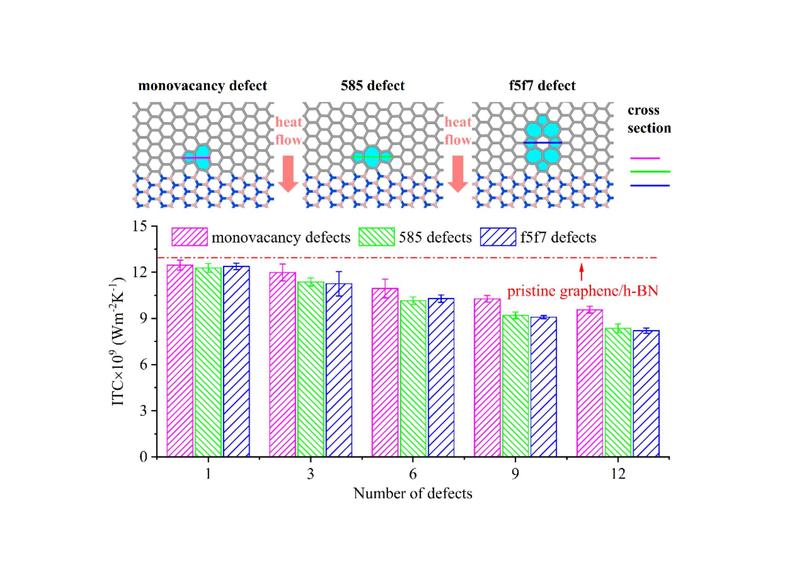
Figure 2. The ITC of pristine graphene/h-BN and graphene/h-BN with different types of defects and number of defects. The inset shows the schematic diagrams and cross sections of the different defects.
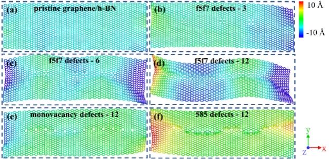
Figure 3. The wrinkles in the near-interface region of pristine graphene/h-BN and graphene/h-BN with intrinsic defects after sufficient relaxation.
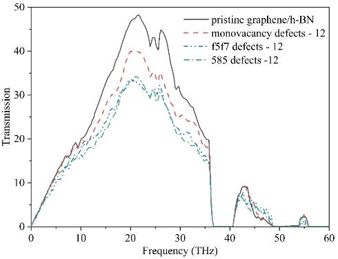
Figure 4. Phonon transmission in the near-interface region of pristine graphene/h-BN and graphene/h-BN with twelve defects.
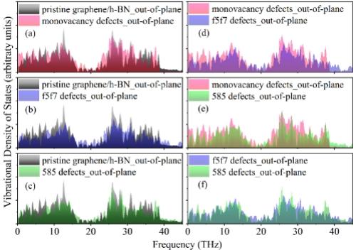
Figure 5. Comparison of the out-of-plane VDOS in the near interface region of pristine graphene/h-BN and defective graphene/h-BN.